Hardware – STEP400
Hardware Overview
PCB size
120x84, thickness = 1.6mm
There are five M3 mounting holes on each four corners and in the middle.
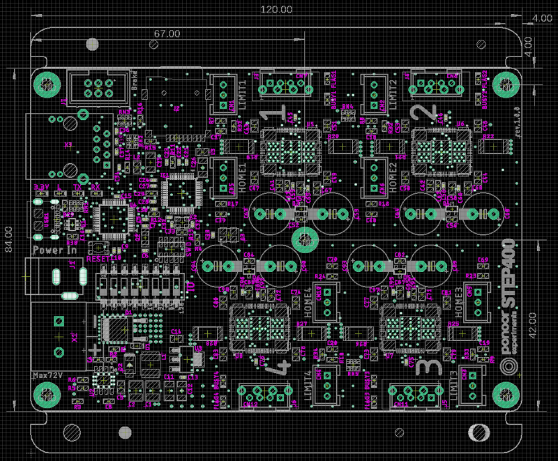 Long parts of the top and bottom in this picture are waste boards, and are removed after the production.
Actual size PDF : step400_r1_dimension.pdf
System
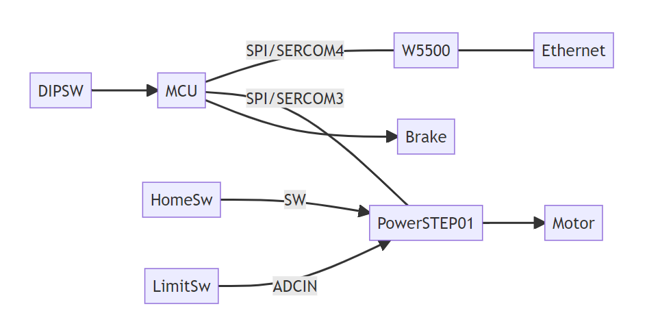
Schematics: step400_r1_schematics.pdf
The main components are as follows;
| Components | Manufacturer | Model number |
|---|---|---|
| MCU | Microchip | ATSAMD21G18A |
| Ethernet Controller | Wiznet | W5500 |
| Stepper Driver | STMicroelectronics | PowerSTEP01 |
| DC-DC Converter | ROHM | BD9G341AEFJ |
Pin assignments
| pin | function | etc |
|---|---|---|
| D0 | DIPSW8 | |
| D1 | Brake4 | |
| D2 | DIPSW5 | |
| D3 | DIPSW7 | |
| D4 | SD_CS | |
| D5 | Brake3 | |
| D6 | PowerSTEP01_MISO | |
| D7 | DIPSW1 | |
| D8 | Brake2 | |
| D9 | DIPSW6 | |
| D10 | W5500_CS | |
| D11 | PowerSTEP01_MOSI | |
| D12 | PowerSTEP01_SCK | |
| D13 | L | |
| D20/SDA | NC | Pad on PCB |
| D21/SCL | NC | Pad on PCB |
| D22/MISO | W5500_MISO | |
| D23/MOSI | W5500_MOSI | |
| D24/SCK | W5500_SCK | |
| D30 | DIPSW2 | |
| D31 | DIPSW4 | |
| D38 | NC | Pad on PCB |
| A0 | PowerSTEP01_CS | |
| A1 | Brake1 | |
| A2 | PowerSTEP01_RESET | |
| A3 | W5500_RESET | |
| A4 | SD_DETECT | |
| A5 | DIPSW3 |
Since the PowerSTEP01_RESET and W5500_RESET are connected to the reset pins of PowerSTEP01 and W5500 individually, be sure to set pinMode to OUTPUT and then set the state to HIGH.
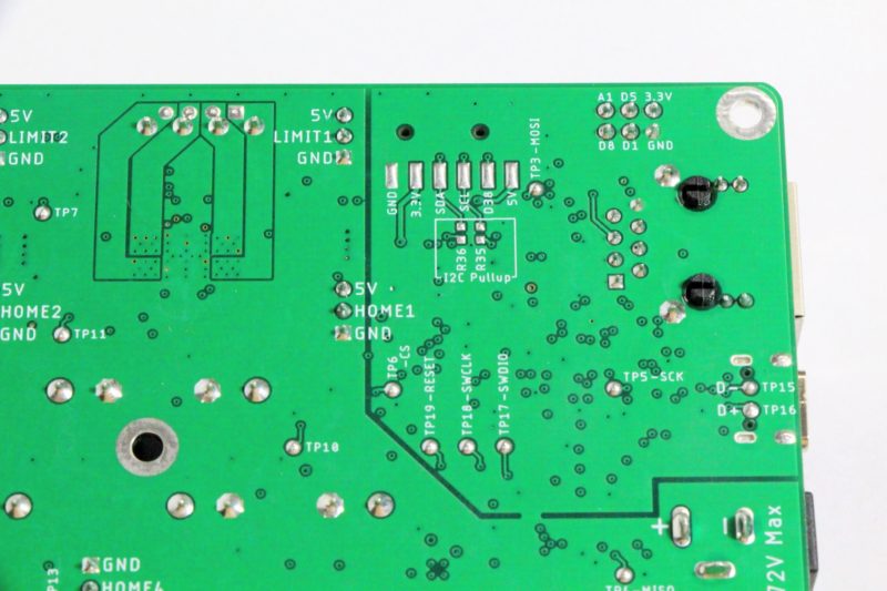
Pads on PCB rear side
There are unassigned pins and power pads on the rear side of PCB. They are 2.54mm picth, so you can attach surface-mount pin-headers and IC sockets. R35 and R36 on the rear side can be used for the pull-up for the i2c pins(SDA, SDL). The chip size is 1608(0603).
Since these pins are not controlled from firmware, customizing firmware for your own purpose is necessary.
SPI assignment
For the STEP400, different SPI ports are used for the PowerSTEP01 and W5500 for the ease of firmware process. Here is a very informative guide to SPI allocation in ATSAMD21.
https://learn.adafruit.com/using-atsamd21-sercom-to-add-more-spi-i2c-serial-ports
W5500
| Pin | Function | SERCOM | SERCOM Alt |
|---|---|---|---|
| D22/MISO | MISO | - | SERCOM4.0 |
| D23/MOSI | MOSI | - | SERCOM4.2 |
| D24/SCK | SCK | - | SERCOM4.3 |
PowerSTEP01
| Pin | Function | SERCOM | SERCOM Alt |
|---|---|---|---|
| D6 | MISO | - | SERCOM3.2 |
| D11 | MOSI | - | SERCOM3.0 |
| D12 | SCK | - | SERCOM3.3 |
PowerSTEP01
Clock
A 16MHz crystal oscillator is connected to the OSCIN of Motor ID 1's PowerSTEP01. From there, OSCOUT and OSCIN are daisy chained in order of IDs, so please set each PowerSTEP01 to "External 16MHz input, Inverted output(EXT_16MHZ_OSCOUT_INVERT)". If the internal clock is used, the movement may shift gradually during constant speed operation.
Unavailable PowerSTEP01 features due to the hardware design
STCK
Since it is not wired, Step Clock operation is not possible.
ADCIN
This is used for the limit sensor inputs, therefore not used for the original supply voltage compensation featue. Be sure to disable UVLO_ADC, which will raise the alarm based on the value of the ADC input.